|
|
|
|
|
||||
|
|
|
|
|
| |||
|
Adding a transformer to a step-up dc-dc regulator enables the regulator to accept inputs of 20V and higher while operating in a flyback step-down mode (Figure 1). The circuit of Figure 1 handles inputs up to 30V (as shown), but is easily modified for higher specific voltages. It was developed for use in a small industrial controller whose non-ventilated case required close attention to power dissipation. 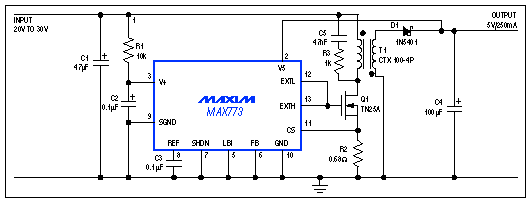 Figure 1. This step-up switching regulator and 1:1 transformer steps down to 5V from input voltages as high as 30V. IC1 is well suited to the application because it drives an external switching transistor and derives its power from an internal shunt regulator?both of which can be made to accommodate a wide range of input voltages. IC1 includes internal feedback resistors for 5V, 12V, or 15V outputs (the connection shown is for 5V). To set output voltages other than these, connect a feedback divider between the circuit's regulated output and IC1's feedback terminal (pin 6). Though not optimal for efficiency, the transformer's 1:1 turns ratio simplifies procurement by allowing the use of a standard product such as the Coiltronix CTX transformer shown. Its 1:1 ratio also enhances stability by producing a duty cycle well below 50%. An ideal 1:1 transformer would generate VIN + VOUT at the bottom of the primary, but leakage inductance causes real transformers to produce a somewhat higher voltage. That voltage appears across Q1, so Q1's minimum breakdown voltage should be approximately 2VIN + VOUT. A snubber network across T1 reduces this breakdown-voltage requirement, at the cost of efficiency. The simplest snubber is the RC network shown in Figure 1. (A zener-diode type allows higher efficiency.) The amount of "snubbing" required depends on the output load, the circuit layout, and the parasitic elements present. For IOUT = 250mA and VIN between 20V and 30V, this circuit's efficiency is 66% (rising to 72% when you remove the snubber). R2 limits the peak current through Q1 and L1 to 0.33A. The internal shunt regulator is a zener diode, biased by R1 at approximately 2mA (the allowed range is 1mA to 20mA). Replacing R1 with a constant-current source lets the circuit cope with a wider input voltage range. The shunt regulator's output is about 6V, which limits the gate drive to Q1; therefore, Q1 should have a logic-level gate threshold. (The VN88 MOSFET also works well, though its 2.5V maximum gate threshold is slightly high for this criterion). The SHDN input (pin 7, shown grounded) is a digital on/off switch for the load and the switching circuit. The shunt regulator remains active during shutdown and provides a useful supply voltage for backup memory, a real-time clock, or any general-purpose logic (including a latching on/off switch). The shunt regulator can supply 4000-series logic directly, or can supply 5V-specified devices via two "dropper" diodes. |
|
PRODUCTS •
DESIGN •
SUPPORT • SALES • ABOUT
MAXIM HOME • EMPLOYMENT • CONTACT US • JAPANESE • CHINESE |
|
Copyright
© 2000 Maxim Integrated Products |